SERVICES OVERVIEW
From concept to mass production, choose the engagement model and capabilities that fit your project. Every path leads to the same outcome: tested, production-ready PCBA boards delivered from our Shenzhen facility.
Find Your Engagement Model
Match your current stage to the right partnership model. Click through for full details on each.
"I have complete Gerber & BOM files."
Your design is released and locked. You need a turnkey PCBA manufacturer that handles comprehensive DFM review, component sourcing from Tier-1 distributors, SMT & THT assembly, inline AOI and X-Ray inspection, and on-time delivery — no design work needed.
"I have a product spec — and a software & AI team."
You write the code; we engineer the hardware. Whether you're shipping an embedded Linux appliance, an AI edge inference device, or an IoT controller, our team handles hardware architecture, SoC selection, schematic design, high-speed PCB layout, and embedded firmware integration — giving your software team a production-ready PCBA without building an in-house hardware department.
"I have a market opportunity and a target price point."
You define the product requirements — we manage the full development lifecycle. Custom PCBA design and PCB layout, BOM optimization, embedded firmware development, optional box-build assembly, and complete certification management (CE, FCC, UL, RoHS). White-label ready: your brand on a packaged, market-ready product.
Turnkey PCBA — Three Core Capabilities
Every engagement model gives you access to our full engineering, manufacturing, and testing stack.
PCB Design & Engineering
Full-stack hardware design — from system architecture and SoC selection to schematic capture, high-speed HDI PCB layout, SI/PI simulation, and embedded firmware (bare-metal, RTOS, Linux). Every design passes DFM/DFT review before release, ensuring seamless transition to manufacturing.
- Schematic & Layout
- Firmware
- DFM/DFT
- NPI
Manufacturing & Assembly
Full turnkey PCB fabrication and SMT assembly: 1–32 layer PCBs with 2.5/2.5 mil HDI, ±5% differential impedance, blind/buried vias, and back drilling; 12,000 m² monthly capacity. SMT: 7 Yamaha lines (YSM20/20R + YSM10) at 300K placements/hour, 48-hour quick-turn >95%, with inline 3D SPI, AOI, and X-Ray. DIP/selective soldering and box-build integration included.
- SMT
- DIP
Testing & Compliance
Custom ICT/FCT fixture design and fabrication. Environmental stress testing — thermal cycling (−55 to +125 °C), 85 °C / 85% RH humidity, vibration (IEC 60068-2-6 / -2-64), and 168-hour burn-in. Design-stage EMC review with partner-lab pre-compliance coordination, plus full certification management for CE, FCC, UKCA, and UL, with RoHS / REACH compliance support.
- ICT/FCT
- EMC/ESD
- CE/FCC
- Reliability
Capabilities × Engagement Models — At a Glance
See how our three core capabilities intersect with each engagement model. Green checkmarks indicate full delivery; blue partial indicates review/advisory scope.
| Capability / Deliverable | OEM / EMS | JDM | ODM |
|---|---|---|---|
| Your Input | Gerber, BOM, assembly drawings | Product definition & concept | PRD, target spec & cost |
| Hardware Design | DFM Review Only | ✓ Co-developed | ✓ We design |
| Firmware Development | Not included | ✓ BSP + low-level by us | ✓ Included |
| BOM Sourcing | Turnkey | Turnkey | Turnkey |
| SMT / DIP Assembly | ✓ In-house | ✓ In-house | ✓ In-house |
| Functional Testing (FCT) | ✓ Per client spec | ✓ Custom fixture dev | ✓ Custom fixture dev |
| Certification Management | By request | Pre-compliance | ✓ Full management |
| Design File Terms | ✓ Client retains (your files) | Flexible — discussed at proposal | Per engagement agreement |
| Engagement Structure | File-to-shipment — defined scope, fixed deliverables | Concept-to-production — phased, iterative co-development | Milestone-driven — PRD to packaged product |
| Minimum Order | 1–50 proto OK | Flexible MOQ | Project-based |
Turnkey PCBA Delivery Workflow
The same proven process applies regardless of engagement model — what changes is where you enter. JDM and ODM start at Step 1; EMS typically enters at Step 3 or 4.
Concept & Architecture
We translate your product vision into a viable technical blueprint — requirements analysis, SoC selection, feasibility assessment, and initial BOM cost estimation to lock in the target budget before a single trace is routed.
Schematic & PCB Layout
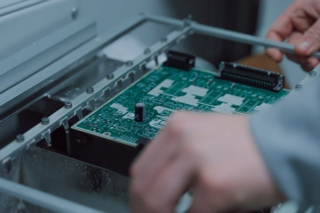
Schematic capture with full DRC, high-speed and HDI PCB routing, SI/PI and thermal simulation. Every design is reviewed for DFM and DFT before release — eliminating costly re-spins downstream.
Prototype & Validation
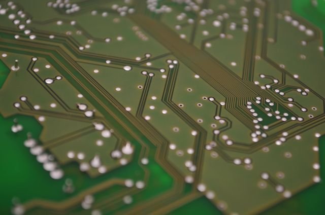
Quick-turn in-house PCBA prototyping (as fast as 48 hours), firmware bring-up and debugging, environmental stress testing, and iterative EVT/DVT cycles until every parameter meets specification.
NPI & Mass Production
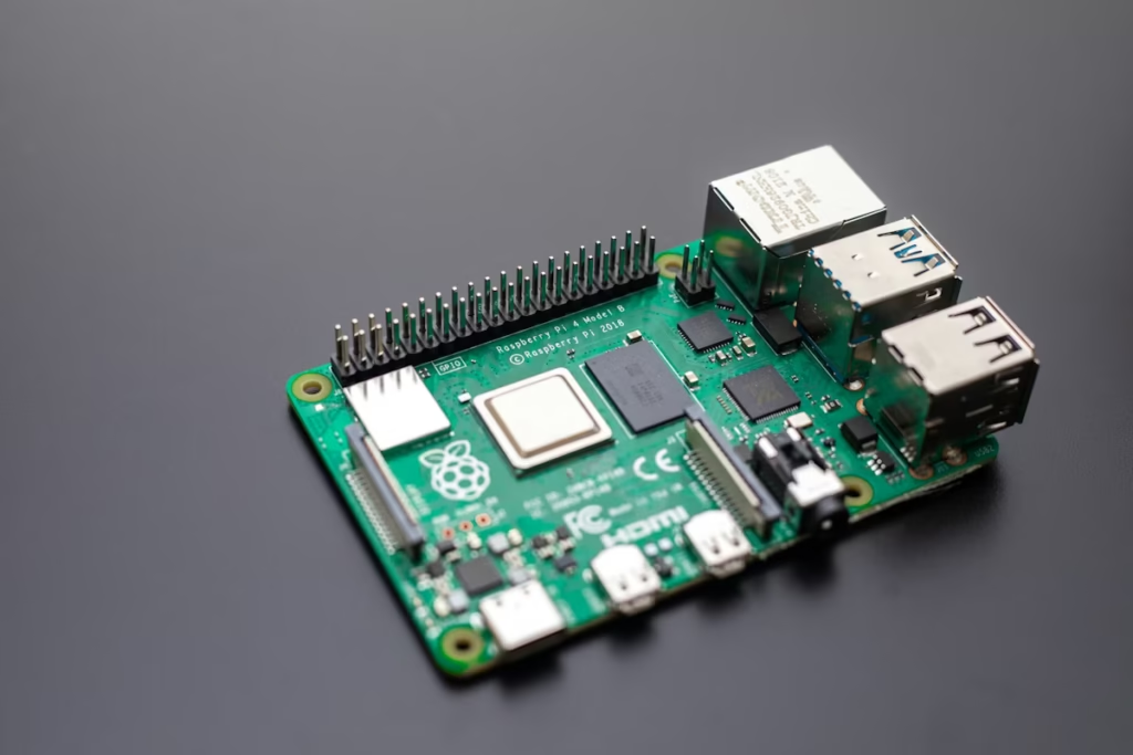
Custom FCT/ICT fixture development, global certification (CE/FCC/RoHS), and seamless NPI transition. Your product moves from engineering samples to volume production with repeatable quality and full traceability.